Ever wondered how engineers determine if the signal traveling through a PCB is precise and accurate? The quality of the signals in PCBs is crucial for high-speed electronics, such as smartphones, computers, and other digital gadgets. An eye diagram is a powerful tool to test this quality. What is an eye chart, and why does the performance of your PCB depend on it? This topic will be explained in plain English so that everyone can understand it.
What is an Eye Diagram?
Imagine watching the waves roll onto a beach. Some waves are large and clear, while others are smaller or mixed with noise. Eye diagrams capture many waveforms of signals over time, and then overlap them into one image. The eye diagram looks like an image of a human eye.
The eye diagrams illustrate how digital signals behave when they move through the PCB. The diagram shows thousands or even millions of signal cycles stacked on top of each other, instead of just looking at one cycle. The overlapping of signals reveals noise, timing mistakes, and signal distortions that are not visible when you look at the individual signals.
Why are Eye Diagrams Necessary in High-Speed PCB design?
Signals move quickly in everyday electronics. Signals are more likely than ever to be distorted or lost as speeds increase. This is due to many factors, such as interference, reflections, or timing issues. Eye diagrams are a valuable tool for many reasons.
- The “eyes” show the clarity of the signal visually. A wide-open eye means that it is easy to differentiate between a “0” and a “1”. Closed or fuzzy eyes indicate a noisy or shaky signal.
- Eye diagrams can help identify signal problems. They reveal issues such as jitter, noise, reflections, and crosstalk. These errors can lead to data failures or device malfunctions.
- They can help improve design: By analyzing eye patterns, engineers can change the layout of the PCB or the materials used to enhance signal quality.
- They are used by industry to meet standards. Eye diagrams help test high-speed interfaces such as USB, HDMI, or Ethernet.
Understanding the key features of an eye diagram
It helps to understand the parts of an eye diagram before you can read it:
The Eye Opening (Width and Height):
The vertical opening shows the voltage margins, or how well the levels “0” and “1” are separated. The larger the horizontal eye, the greater the timing margin. This means that the signal will arrive at the correct time.
Jitter:
Jitter is a slight variation or movement in the timing of a signal. When the edges of the signal move to the left or the right, this can cause errors in the reading of digital data.
Noise:
Noise causes the vertical signal to fluctuate, causing the eye level to be reduced and errors.
Crossing points:
The engineers can tell if the timing of the signals is balanced by observing where the signal crosses in the middle.
Multi-Transitions and Ringing
Eye diagrams with extra “paths” and oscillations can be indicative of issues such as crosstalk or reflections within the PCB.
How do engineers use eye diagrams for PCB design?
Engineers use eye diagrams throughout the PCB design, testing, and development process.
1. Pre-Layout simulations
Software is used to simulate eye diagrams before the PCB can be made. It is possible to predict the performance of signals based on design rules, trace lengths, and materials.
2. Post-Layout Test
Engineers capture eye diagrams with oscilloscopes after the PCB has been built. These real results are compared to simulations in order to determine if the design is working as expected or if any changes need to be made.
3. Troubleshooting Signal Integrity
Engineers use the eye diagram when a PCB is not performing well. They can identify issues like jitter or crosstalk. This is like using a chart to diagnose a problem.
The Eye Diagrams Reveal Common Signal Integrity Issues
- Insertion loss: The signal energy decreases as it passes through connectors and traces, particularly with long paths. This reduces the opening of the eye.
- Inter-Symbol Interference: Signals that blur or overlap due to limited bandwidth, or materials with lossy quality. This causes the eyelids to close.
- Crosstalk: Signals interfered with by nearby traces, distorting eye shape.
- Reflections and Impedance mismatch: Abrupt changes to transmission line characteristics can cause ripples or echoes in the signals.
- Jitter: Timing fluctuations may cause the eye to close horizontally.
- Ringing: Sharp edges can cause oscillations that affect the signal quality.
Tips to Improve Eye Diagrams in PCB Layout and Signal Integrity
If you want a clear eye diagram–and ultimately, reliable signal performance–consider these practical PCB design tips:
- Use controlled impedance traces: By matching impedance, you can prevent reflections and ringing.
- Avoid prolonged or convoluted paths as they can reduce signal strength.
- Avoid sharp bends: Curved traces have a consistent impedance.
- Separate signal traces: Reduce crosstalk between lines by spacing them apart.
- Use proper grounding and shielding to reduce noise and interference.
- Minimize Via Usage: Every via can introduce signal degradation.
- Test Early and Simulate Often. Use real measurements and signal integrity tools to catch problems early.
Eye Diagrams in Real Life: A Case Study
Imagine a conversation taking place in a loud room. It isn’t easy to understand if voices are echoed or overlapped. Your device will also struggle to “hear the right signals” if PCB signals are distorted.
Engineers rely on eye charts to ensure that data is transferred without error in devices such as 5G or USB high-speed. Closed eyes would result in a connection that is slow or unreliable, frustrating users and damaging the product’s reputation.
Conclusion
The eye diagrams act as “health reports” on high-speed PCBs. These diagrams give engineers an easy way to see if the signals are timed and clean. They allow engineers to check for issues such as jitter or noise visually.
Understanding and using eye diagrams are key to ensuring strong PCB signals, whether you’re designing for a smartphone or a medical device. It is essential to work closely with your PCB manufacturer and PCB assembly firm in order to ensure that your PCB layout provides clear signals and reliable performance.
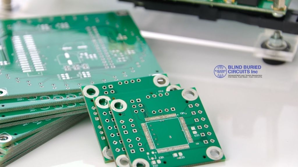
Blind Buried Circuits emphasizes signal quality at every stage of PCB assembly and manufacturing, helping you to achieve optimal eye diagrams as well as top signal integrity for your products.
The Key Takeaways
- The eye diagrams show the quality of digital signals at high speed on PCBs.
- Wide-open eyes indicate clear signals. Closed/skewed eyes point to problems.
- Engineers use eye diagrams to diagnose signal problems such as jitter, noise, and crosstalk.
- The eye diagram and signal integrity of PCBs can be improved by using good PCB design techniques.
- Your design will meet high-speed requirements if you work with a PCB manufacturer.
These insights will help you better understand the importance of eye diagrams for your next PCB design.